Texas Instruments
ADC12C080CISQ/NOPB
ADC12C080CISQ/NOPB
Couldn't load pickup availability
ADC12C080CISQ/NOPB Texas Instruments - Yeehing Electronics
12-Bit, 80-MSPS, 1.0-GHz Input Bandwidth Analog-to-Digital Converter (ADC)
Pricing (USD)
| Quantity | Unit Price |
| 1 — 99 | 26.959 |
| 100 — 249 | 23.963 |
| 250 — 999 | 19.699 |
| 1,000 + | 12.33 |
The above prices are for reference only.
Specifications
| Manufacturer | Texas Instruments |
| Product Category | Analog to Digital Converters - ADC |
| RoHS | Y |
| Series | ADC12C080 |
| Mounting Style | SMD/SMT |
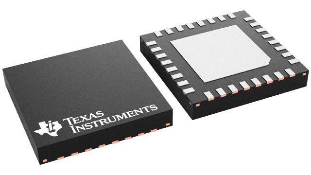
| Package / Case | WQFN-32 |
| Resolution | 12 bit |
| Number of Channels | 1 Channel |
| Sampling Rate | 80 MS/s |
| Input Type | Differential |
| Interface Type | Parallel |
| Architecture | Pipeline |
| Reference Type | External, Internal |
| Analog Supply Voltage | 2.7 V to 3.6 V |
| Digital Supply Voltage | 2.4 V to 3.6 V |
| SNR - Signal to Noise Ratio | 71.2 dB |
| Minimum Operating Temperature | - 40 C |
| Maximum Operating Temperature | + 85 C |
| Packaging | Reel |
| Features | Low Power |
| Height | 0.8 mm |
| Input Voltage | 2 V |
| Length | 5 mm |
| Number of Converters | 1 Converter |
| Power Consumption | 300 mW |
| Type | S/H ADC |
| Width | 5 mm |
| Brand | Texas Instruments |
| Development Kit | ADC12C080EB/NOPB |
| DNL - Differential Nonlinearity | +/- 0.35 LSB |
| ENOB - Effective Number of Bits | 11.1 Bit |
| INL - Integral Nonlinearity | 0.5 LSB |
| Moisture Sensitive | Yes |
| Number of ADC Inputs | 1 Input |
| Operating Supply Voltage | 3 V |
| Pd - Power Dissipation | 300 mW |
| Product Type | ADCs - Analog to Digital Converters |
| Sample and Hold | Yes |
| SFDR - Spurious Free Dynamic Range | 90 dB |
| SINAD - Signal to Noise and Distortion Ratio | 68.5 dB |
| Factory Pack Quantity | 1000 |
| Subcategory | Data Converter ICs |
For more information, please refer to datasheet
Documents
| ADC12C080CISQ/NOPB Datasheet |
More Information
The ADC12C080 is a high-performance CMOS analog-to-digital converter capable of converting analog input signals into 12-bit digital words at rates up to 80 Mega Samples Per Second (MSPS). This converter uses a differential, pipelined architecture with digital error correction and an on-chip sample-and-hold circuit to minimize power consumption and the external component count, while providing excellent dynamic performance. A unique sample-and-hold stage yields a full-power bandwidth of 1 GHz. The ADC12C080 may be operated from a single +3.0V power supply and consumes low power. A separate +2.5V supply may be used for the digital output interface which allows lower power operation with reduced noise. A power-down feature reduces the power consumption to very low levels while still allowing fast wake-up time to full operation. The differential inputs accept a 2V full scale differential input swing. A stable 1.2V internal voltage reference is provided, or the ADC12C080 can be operated with an external 1.2V reference. Output data format (offset binary versus 2's complement) and duty cycle stabilizer are pin-selectable. The duty cycle stabilizer maintains performance over a wide range of clock duty cycles.

