Texas Instruments
ADC12DS080CISQE/NOPB
ADC12DS080CISQE/NOPB
Couldn't load pickup availability
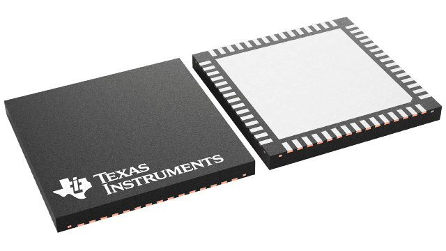
ADC12DS080CISQE/NOPB Texas Instruments - Yeehing Electronics
Dual-Channel, 12-Bit, 80-MSPS Analog-to-Digital Converter (ADC)
Pricing (USD)
| Quantity | Unit Price |
| 1 — 99 | 41.234 |
| 100 — 249 | 36.652 |
| 250 — 999 | 30.13 |
| 1,000 + | 18.86 |
The above prices are for reference only.
Specifications
| Manufacturer | Texas Instruments |
| Product Category | Analog to Digital Converters - ADC |
| RoHS | Y |
| Series | ADC12DS080 |
| Mounting Style | SMD/SMT |
| Package / Case | WQFN-60 |
| Resolution | 12 bit |
| Number of Channels | 2 Channel |
| Sampling Rate | 80 MS/s |
| Input Type | Differential |
| Interface Type | Serial |
| Architecture | Pipeline |
| Reference Type | External, Internal |
| Analog Supply Voltage | 2.7 V to 3.6 V |
| Digital Supply Voltage | 2.7 V to 3.6 V |
| SNR - Signal to Noise Ratio | 71 dB |
| Minimum Operating Temperature | - 40 C |
| Maximum Operating Temperature | + 85 C |
| Packaging | Reel |
| Features | Low Power |
| Height | 0.8 mm |
| Input Voltage | 2 V |
| Length | 9 mm |
| Number of Converters | 2 Converter |
| Output Type | LVDS |
| Power Consumption | 800 mW |
| Type | S/H ADC |
| Width | 9 mm |
| Brand | Texas Instruments |
| DNL - Differential Nonlinearity | +/- 0.25 LSB |
| ENOB - Effective Number of Bits | 11.3 Bit |
| Gain Error | 1 % FSR |
| INL - Integral Nonlinearity | 1.5 LSB |
| Moisture Sensitive | Yes |
| Number of ADC Inputs | 2 Input |
| Operating Supply Voltage | 3 V |
| Pd - Power Dissipation | 845 mW |
| Product Type | ADCs - Analog to Digital Converters |
| Sample and Hold | Yes |
| SFDR - Spurious Free Dynamic Range | 81 dB |
| SINAD - Signal to Noise and Distortion Ratio | 69.6 dB |
| Factory Pack Quantity | 250 |
| Subcategory | Data Converter ICs |
For more information, please refer to datasheet
Documents
| ADC12DS080CISQE/NOPB Datasheet |
More Information
The ADC12DS080 is a high-performance CMOS analog-to-digital converter capable of converting two analog input signals into 12-bit digital words at rates up to 80 Mega Samples Per Second (MSPS). The digital outputs are serialized and provided on differential LVDS signal pairs. This converter uses a differential, pipelined architecture with digital error correction and an on-chip sample-and-hold circuit to minimize power consumption and the external component count, while providing excellent dynamic performance. The ADC12DS080 may be operated from a single +3.0V or 3.3V power supply. A power-down feature reduces the power consumption to very low levels while still allowing fast wake-up time to full operation. The differential inputs accept a 2V full scale differential input swing. A stable 1.2V internal voltage reference is provided, or the ADC12DS080 can be operated with an external 1.2V reference. The selectable duty cycle stabilizer maintains performance over a wide range of clock duty cycles. A serial interface allows access to the internal registers for full control of the ADC12DS080's functionality. The ADC12DS080 is available in a 60-lead WQFN package and operates over the industrial temperature range of −40°C to +85°C

