Texas Instruments
ADC16DV160CILQ/NOPB
ADC16DV160CILQ/NOPB
Couldn't load pickup availability
ADC16DV160CILQ/NOPB Texas Instruments - Yeehing Electronics
Dual-Channel, 16-Bit, 160-MSPS Analog-to-Digital Converter (ADC)
Pricing (USD)
| Quantity | Unit Price |
| 1 — 99 | 135.674 |
| 100 — 249 | 122.808 |
| 250 — 999 | 119.299 |
| 1,000 + | 81.87 |
The above prices are for reference only.
Specifications
| Manufacturer | Analog Devices Inc. |
| Product Category | Analog to Digital Converters - ADC |
| RoHS | Y |
| Series | AD7887 |
| Mounting Style | SMD/SMT |
| Package / Case | MSOP-8 |
| Resolution | 12 bit |
| Number of Channels | 2 Channel |
| Sampling Rate | 125 kS/s |
| Input Type | Single-Ended |
| Interface Type | SPI |
| Architecture | SAR |
| Reference Type | External, Internal |
| SNR - Signal to Noise Ratio | 71 dB |
| Minimum Operating Temperature | - 40 C |
| Maximum Operating Temperature | + 125 C |
| Qualification | AEC-Q100 |
| Packaging | Reel |
| Height | 0.85 mm |
| Input Voltage | 2.5 V |
| Length | 3 mm |
| Number of Converters | 1 Converter |
| Type | S/H ADC |
| Width | 3 mm |
| Brand | Analog Devices |
| Development Kit | EVAL-AD7887CBZ |
| DNL - Differential Nonlinearity | +/- 2 LSB |
| Gain Error | +/- 2 LSB |
| INL - Integral Nonlinearity | +/- 2 LSB |
| Number of ADC Inputs | 1 Input/2 Input |
| Operating Supply Voltage | 5 V |
| Pd - Power Dissipation | 3.5 mW |
| Product Type | ADCs - Analog to Digital Converters |
| Sample and Hold | Yes |
| Factory Pack Quantity | 3000 |
| Subcategory | Data Converter ICs |
| Unit Weight | 0.004938 oz |
For more information, please refer to datasheet
Documents
| ADC16DV160CILQ/NOPB Datasheet |
More Information
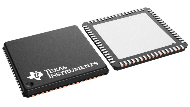
The ADC16DV160 is a monolithic dual channel high performance CMOS analog-to-digital converter capable of converting analog input signals into 16-bit digital words at rates up to 160 Mega Samples Per Second (MSPS). This converter uses a differential, pipelined architecture with digital error correction and an on-chip sample-and-hold circuit to minimize power consumption and external component count while providing excellent dynamic performance. Automatic power-up calibration enables excellent dynamic performance and reduces part-to-part variation, and the ADC16DV160 can be re-calibrated at any time through the 3-wire Serial Peripheral Interface (SPI). An integrated low noise and stable voltage reference and differential reference buffer amplifier eases board level design. The on-chip duty cycle stabilizer with low additive jitter allows a wide range of input clock duty cycles without compromising dynamic performance. A unique sample-and-hold stage yields a full-power bandwidth of 1.4 GHz. The interface between the ADC16DV160 and a receiver block can be easily verified and optimized via fixed pattern generation and output clock position features. The digital data is provided via dual data rate LVDS outputs – making possible the 68-pin, 10 mm x 10 mm VQFN package. The ADC16DV160 operates on dual power supplies of +1.8V and +3.0V with a power-down feature to reduce power consumption to very low levels while allowing fast recovery to full operation.