Texas Instruments
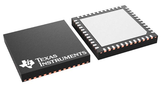
ADC3244IRGZR
ADC3244IRGZR
Couldn't load pickup availability
ADC3244IRGZR Texas Instruments - Yeehing Electronics
Dual-channel 14-bit 125-MSPS analog-to-digital converter (ADC)
Pricing (USD)
| Quantity | Unit Price |
| 1 — 99 | 40.574 |
| 100 — 249 | 36.066 |
| 250 — 999 | 29.648 |
| 1,000 + | 18.56 |
The above prices are for reference only.
Specifications
| Manufacturer | Texas Instruments |
| Product Category | Analog to Digital Converters - ADC |
| RoHS | Y |
| Series | ADC3244 |
| Mounting Style | SMD/SMT |
| Package / Case | VQFN-48 |
| Resolution | 14 bit |
| Number of Channels | 2 Channel |
| Sampling Rate | 125 MS/s |
| Input Type | Differential |
| Interface Type | Serial LVDS |
| Architecture | Pipeline |
| Reference Type | External, Internal |
| Analog Supply Voltage | 1.8 V |
| Digital Supply Voltage | 1.8 V |
| SNR - Signal to Noise Ratio | 73.1 dB |
| Minimum Operating Temperature | - 40 C |
| Maximum Operating Temperature | + 85 C |
| Packaging | Reel |
| Features | Low Power |
| Input Voltage | 2 Vp-p |
| Number of Converters | 2 Converter |
| Output Type | LVDS |
| Power Consumption | 232 mW |
| Type | High Speed ADC |
| Brand | Texas Instruments |
| ENOB - Effective Number of Bits | 11.8 Bit |
| Moisture Sensitive | Yes |
| Operating Supply Voltage | 1.7 V to 1.9 V |
| Pd - Power Dissipation | 325 mW |
| Product Type | ADCs - Analog to Digital Converters |
| SFDR - Spurious Free Dynamic Range | 93 dB |
| SINAD - Signal to Noise and Distortion Ratio | 73 dB |
| Factory Pack Quantity | 2500 |
| Subcategory | Data Converter ICs |
| Unit Weight | 0.004868 oz |
For more information, please refer to datasheet
Documents
| ADC3244IRGZR Datasheet |
More Information
The ADC324x are a high-linearity, ultra-low power, dual-channel, 14-bit, 25-MSPS to 125-MSPS, analog-to-digital converter (ADC) family. The devices are designed specifically to support demanding, high input frequency signals with large dynamic range requirements. An input clock divider allows more flexibility for system clock architecture design and the SYSREF input enables complete system synchronization. The ADC324x family supports serial low-voltage differential signaling (LVDS) in order to reduce the number of interface lines, thus allowing for high system integration density. The serial LVDS interface is two-wire, where each ADC data are serialized and output over two LVDS pairs. An internal phase-locked loop (PLL) multiplies the incoming ADC sampling clock to derive the bit clock that is used to serialize the 14-bit output data from each channel. In addition to the serial data streams, the frame and bit clocks are also transmitted as LVDS outputs.

