Texas Instruments
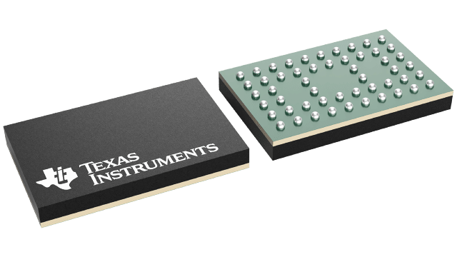
CDCU877ANMKT
CDCU877ANMKT
Couldn't load pickup availability
CDCU877ANMKT Texas Instruments - Yeehing Electronics
1.8-V phase-lock loop clock driver for DDR2 SDRAM applications
Pricing (USD)
| Quantity | Unit Price |
| 1 — 99 | 8.9 |
| 100 — 249 | 7.256 |
| 250 — 999 | 5.703 |
| 1,000 + | 3.39 |
The above prices are for reference only.
Specifications
For more information, please refer to datasheet
Documents
| CDCU877ANMKT Datasheet |
More Information
The CDCU877 is a high-performance, low-jitter, low-skew, zero-delay buffer that distributes a differential clock input pair (CK, CK) to ten differential pairs of clock outputs (Yn, Yn) and to one differential pair of feedback clock outputs (FBOUT, FBOUT). The clock outputs are controlled by the input clocks (CK, CK), the feedback clocks (FBIN, FBIN), the LVCMOS control pins (OE, OS), and the analog power input (AVDD). When OE is low, the clock outputs, except FBOUT/FBOUT, are disabled while the internal PLL continues to maintain its locked-in frequency. OS (output select) is a program pin that must be tied to GND or VDD. When OS is high, OE functions as previously described. When OS and OE are both low, OE has no affect on Y7/Y7, they are free running. When AVDD is grounded, the PLL is turned off and bypassed for test purposes.