Texas Instruments
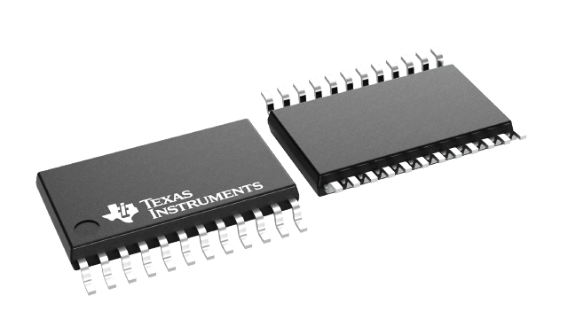
CDCVF2310MPWEP
CDCVF2310MPWEP
Couldn't load pickup availability
CDCVF2310MPWEP Texas Instruments - Yeehing Electronics
Enhanced Product 2.5-V to 3.3-V high performance clock buffer
Pricing (USD)
| Quantity | Unit Price |
| 1 — 99 | 11.992 |
| 100 — 249 | 10.475 |
| 250 — 999 | 8.076 |
| 1,000 + | 5.06 |
The above prices are for reference only.
Specifications
| Manufacturer | Texas Instruments |
| Product Category | Clock Buffer |
| RoHS | N |
| Series | CDCVF2310-EP |
| Number of Outputs | 10 Output |
| Maximum Input Frequency | 200 MHz |
| Supply Voltage - Max | 3.6 V |
| Supply Voltage - Min | 2.3 V |
| Minimum Operating Temperature | - 55 C |
| Maximum Operating Temperature | + 125 C |
| Mounting Style | SMD/SMT |
| Package / Case | TSSOP-24 |
| Packaging | Tube |
| Input Type | LVTTL |
| Output Type | LVTTL |
| Brand | Texas Instruments |
| Max Output Freq | 200 MHz |
| Operating Supply Current | 5 uA |
| Product Type | Clock Buffer |
| Factory Pack Quantity | 60 |
| Subcategory | Clock & Timer ICs |
| Part # Aliases | V62/13603-01XE-T |
| Unit Weight | 0.007478 oz |
For more information, please refer to datasheet
Documents
| CDCVF2310MPWEP Datasheet |
More Information
The CDCVF2310 is a high-performance, low-skew clock buffer that operates up to 200 MHz. Two banks of five outputs each provide low-skew copies of CLK. After power up, the default state of the outputs is low regardless of the state of the control pins. For normal operation, the outputs of bank 1Y[0:4] or 2Y[0:4] can be placed in a low state when the control pins (1G or 2G, respectively) are held low and a negative clock edge is detected on the CLK input. The outputs of bank 1Y[0:4] or 2Y[0:4] can be switched into the buffer mode when the control pins (1G and 2G) are held high and a negative clock edge is detected on the CLK input. The device operates in a 2.5-V and 3.3-V environment. The built-in output enable glitch suppression ensures a synchronized output enable sequence to distribute full period clock signals.

