Texas Instruments
CDCVF855PW
CDCVF855PW
Couldn't load pickup availability
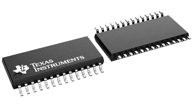
CDCVF855PW Texas Instruments - Yeehing Electronics
2.5-V phase lock loop DDR clock driver
Pricing (USD)
| Quantity | Unit Price |
| 1 — 99 | 3.715 |
| 100 — 249 | 3.029 |
| 250 — 999 | 2.38 |
| 1,000 + | 1.41 |
The above prices are for reference only.
Specifications
| Manufacturer | Texas Instruments |
| Product Category | Clock Drivers & Distribution |
| RoHS | Y |
| Series | CDCVF855 |
| Supply Voltage - Max | 2.7 V |
| Supply Voltage - Min | 2.18 V |
| Minimum Operating Temperature | - 40 C |
| Maximum Operating Temperature | + 85 C |
| Mounting Style | SMD/SMT |
| Package / Case | TSSOP-28 |
| Packaging | Reel |
| Height | 1.15 mm |
| Length | 9.7 mm |
| Type | Zero Delay PLL Clock Driver |
| Width | 4.4 mm |
| Brand | Texas Instruments |
| Product Type | Clock Drivers & Distribution |
| Factory Pack Quantity | 2000 |
| Subcategory | Clock & Timer ICs |
| Unit Weight | 0.004145 oz |
For more information, please refer to datasheet
Documents
| CDCVF855PW Datasheet |
More Information
The CDCVF855 is a high-performance, low-skew, low-jitter, zero-delay buffer that distributes a differential clock input pair (CLK, CLK) to 4 differential pairs of clock outputs (Y[0:3], Y[0:3]) and one differential pair of feedback clock outputs (FBOUT, FBOUT). The clock outputs are controlled by the clock inputs (CLK, CLK), the feedback clocks (FBIN, FBIN), and the analog power input (AVDD). When PWRDWN is high, the outputs switch in phase and frequency with CLK. When PWRDWN is low, all outputs are disabled to a high-impedance state (3-state) and the PLL is shut down (low-power mode). The device also enters this low-power mode when the input frequency falls below a suggested detection frequency that is below 20 MHz (typical 10 MHz). An input frequency-detection circuit detects the low-frequency condition and, after applying a >20-MHz input signal, this detection circuit turns the PLL on and enables the outputs.

