Texas Instruments
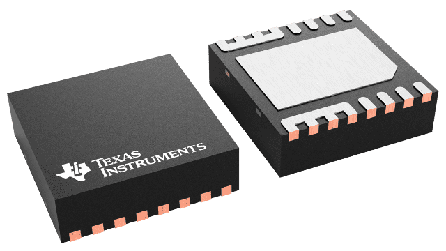
CSD95379Q3MT
CSD95379Q3MT
Couldn't load pickup availability
CSD95379Q3MT Texas Instruments - Yeehing Electronics
Synchronous Buck NexFET Power Stage, CSD95379Q3M
Pricing (USD)
| Quantity | Unit Price |
| 1 — 99 | 1.581 |
| 100 — 249 | 1.306 |
| 250 — 999 | 0.938 |
| 1,000 + | 0.49 |
The above prices are for reference only.
Specifications
| Manufacturer | Texas Instruments |
| Product Category | Gate Drivers |
| RoHS | N |
| Product | MOSFET Gate Drivers |
| Type | High Side, Low Side |
| Mounting Style | SMD/SMT |
| Package / Case | VSON-10 |
| Number of Drivers | 2 Driver |
| Number of Outputs | 2 Output |
| Output Current | 20 A |
| Rise Time | 60 ns |
| Fall Time | 60 ns |
| Supply Voltage - Min | 4.5 V |
| Supply Voltage - Max | 5.5 V |
| Operating Supply Current | 5.5 mA |
| Pd - Power Dissipation | 6 W |
| Minimum Operating Temperature | - 40 C |
| Maximum Operating Temperature | + 150 C |
| Series | CSD95379Q3M |
| Packaging | Reel |
| Operating Temperature Range | - 40 C to + 150 C |
| Technology | Si |
| Brand | Texas Instruments |
| Moisture Sensitive | Yes |
| Product Type | Gate Drivers |
| Factory Pack Quantity | 250 |
| Subcategory | PMIC - Power Management ICs |
| Tradename | NexFET |
| Unit Weight | 0.001213 oz |
For more information, please refer to datasheet
Documents
| CSD95379Q3MT Datasheet |
More Information
The CSD95379Q3M NexFET™ power stage is a highly optimized design for use in high-power, high-density synchronous buck converters. This product integrates the driver IC and NexFET technology to complete the power stage switching function. The driver IC has a built-in selectable diode emulation function that enables DCM operation to improve light load efficiency. In addition, the driver IC supports ULQ mode that enables Connected Standby for Windows® 8. With the PWM input in tri-state, quiescent current is reduced to 130 µA, with immediate response. When SKIP# is held at tri-state, the current is reduced to 8 µA (typically 20 µs is required to resume switching). This combination produces high-current, high-efficiency, and high-speed switching capability in a small 3.3-mm × 3.3-mm outline package. In addition, the PCB footprint has been optimized to help reduce design time and simplify the completion of the overall system design.