Texas Instruments
DS90C387RVJD/NOPB
DS90C387RVJD/NOPB
Couldn't load pickup availability
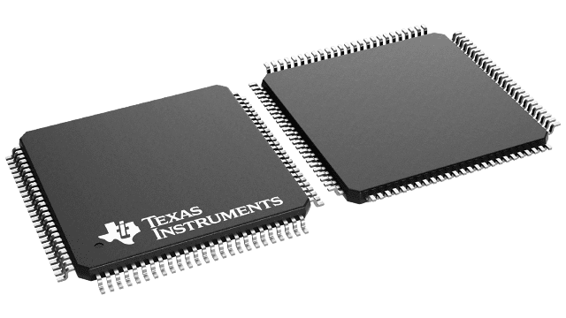
DS90C387RVJD/NOPB Texas Instruments - Yeehing Electronics
85MHz Dual 12-Bit Double Pumped Input LDI Transmitter VGA/UXGA
Pricing (USD)
| Quantity | Unit Price |
| 1 — 99 | 8.046 |
| 100 — 249 | 7.028 |
| 250 — 999 | 5.419 |
| 1,000 + | 3.39 |
The above prices are for reference only.
Specifications
| Manufacturer | Texas Instruments |
| Product Category | LVDS Interface IC |
| RoHS | Y |
| Type | LVCMOS, LVTTL |
| Number of Drivers | 8 Driver |
| Number of Receivers | 24 Receiver |
| Data Rate | 4760 Mb/s |
| Input Type | LVCMOS |
| Supply Voltage - Max | 3.6 V |
| Supply Voltage - Min | 3 V |
| Minimum Operating Temperature | - 10 C |
| Maximum Operating Temperature | + 70 C |
| Mounting Style | SMD/SMT |
| Package / Case | TQFP-100 |
| Packaging | Tray |
| Height | 1 mm |
| Input Voltage MAX | 2 V |
| Length | 14 mm |
| Series | DS90C387R |
| Width | 14 mm |
| Brand | Texas Instruments |
| Input Voltage MIN | 0.8 V |
| Maximum Output Voltage | 550 mV |
| Moisture Sensitive | Yes |
| Operating Supply Voltage | 3.3 V |
| Pd - Power Dissipation | 2.8 W |
| Product Type | LVDS Interface IC |
| Factory Pack Quantity | 90 |
| Subcategory | Interface ICs |
| Unit Weight | 0.023175 oz |
For more information, please refer to datasheet
Documents
| DS90C387RVJD/NOPB Datasheet |
More Information
The DS90C387R transmitter is designed to support pixel data transmission from a Host to a Flat Panel Display up to UXGA resolution. It is designed to be compatible with Graphics Memory Controller Hub (GMCH) by implementing two data per clock and can be controlled by a two-wire serial communication interface. Two input modes are supported: one port of 12-bit( two data per clock) input for 24-bit RGB, and two ports of 12-bit( two data per clock) input for dual 24-bit RGB( 48-bit total). In both modes, input data will be clocked on both rising and falling edges in LVTTL level operation, or clocked on the cross over of differential clock signals in the low swing operation. Each input data width will be 1/2 of clock cycle. With an input clock at 85MHz and input data at 170Mbps, the maximum transmission rate of each LVDS line is 595Mbps, for a aggregate throughput rate of 2.38Gbps/4.76Gbps. It converts 24/48 bits (Single/Dual Pixel 24-bit color) of data into 4/8 LVDS (Low Voltage Differential Signaling) data streams. DS90C387R can be programmed via the two-wire serial communication interface. The LVDS output pin-out is identical to DS90C387. Thus, this transmitter can be paired up with DS90CF388, receiver of the 112MHz LDI chipset or FPD-Link Receivers in non-DC Balance mode operation which provides GUI/LCD panel/mother board vendors a wide choice of inter-operation with LVDS based TFT panels.

