Texas Instruments
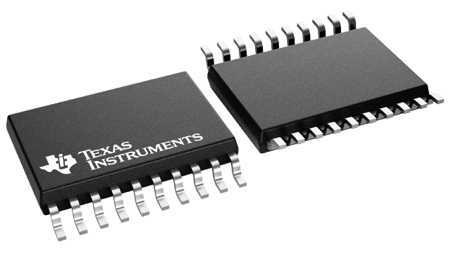
SN74GTLP1395PWR
SN74GTLP1395PWR
Couldn't load pickup availability
SN74GTLP1395PWR Texas Instruments - Yeehing Electronics
Two 1-Bit LVTTL/GTLP Adj-Edge-Rate Bus Xcvrs w Split LVTTL Port, Fdbk Path and Selectable Polarity
Pricing (USD)
| Quantity | Unit Price |
| 1 — 99 | 3.137 |
| 100 — 249 | 2.749 |
| 250 — 999 | 1.927 |
| 1,000 + | 1.09 |
The above prices are for reference only.
Specifications
| Manufacturer | Texas Instruments |
| Product Category | Translation - Voltage Levels |
| RoHS | Y |
| Propagation Delay Time | 9.7 ns |
| Supply Voltage - Max | 3.45 V |
| Supply Voltage - Min | 3.15 V |
| Minimum Operating Temperature | - 40 C |
| Maximum Operating Temperature | + 85 C |
| Mounting Style | SMD/SMT |
| Package / Case | TSSOP-20 |
| Packaging | Reel |
| Features | Partial power down (Ioff), Over-voltage tolerant inputs, Power up 3 state, Bias Vcc, Variable outpu |
| Operating Temperature Range | - 40 C to + 85 C |
| Series | SN74GTLP1395 |
| Brand | Texas Instruments |
| Logic Family | GTLP |
| Operating Supply Current | 20 mA |
| Product Type | Translation - Voltage Levels |
| Factory Pack Quantity | 2000 |
| Subcategory | Logic ICs |
| Unit Weight | 0.002716 oz |
For more information, please refer to datasheet
Documents
| SN74GTLP1395PWR Datasheet |
More Information
The SN74GTLP1395 is two 1-bit, high-drive, 3-wire bus transceivers that provide LVTTL-to-GTLP and GTLP-to-LVTTL signal-level translation for applications, such as primary and secondary clocks, that require individual output-enable and true/complement controls. The device allows for transparent and inverted transparent modes of data transfer with separate LVTTL input and LVTTL output pins, which provide a feedback path for control and diagnostics monitoring. The device provides a high-speed interface between cards operating at LVTTL logic levels and a backplane operating at GTLP signal levels and is designed especially to work with the Texas Instruments 3.3-V 1394 backplane physical-layer controller. High-speed (about three times faster than standard LVTTL or TTL) backplane operation is a direct result of GTLP reduced output swing (<1 V), reduced input threshold levels, improved differential input, OEC circuitry, and TI-OPC circuitry. Improved GTLP OEC and TI-OPC circuitry minimizes bus settling time, and have been designed and tested using several backplane models. The high drive allows incident-wave switching in heavily loaded backplanes, with equivalent load impedance down to 11 .

